Our Process for Engineering Collaboration
Step 1: Getting to Know your Goals
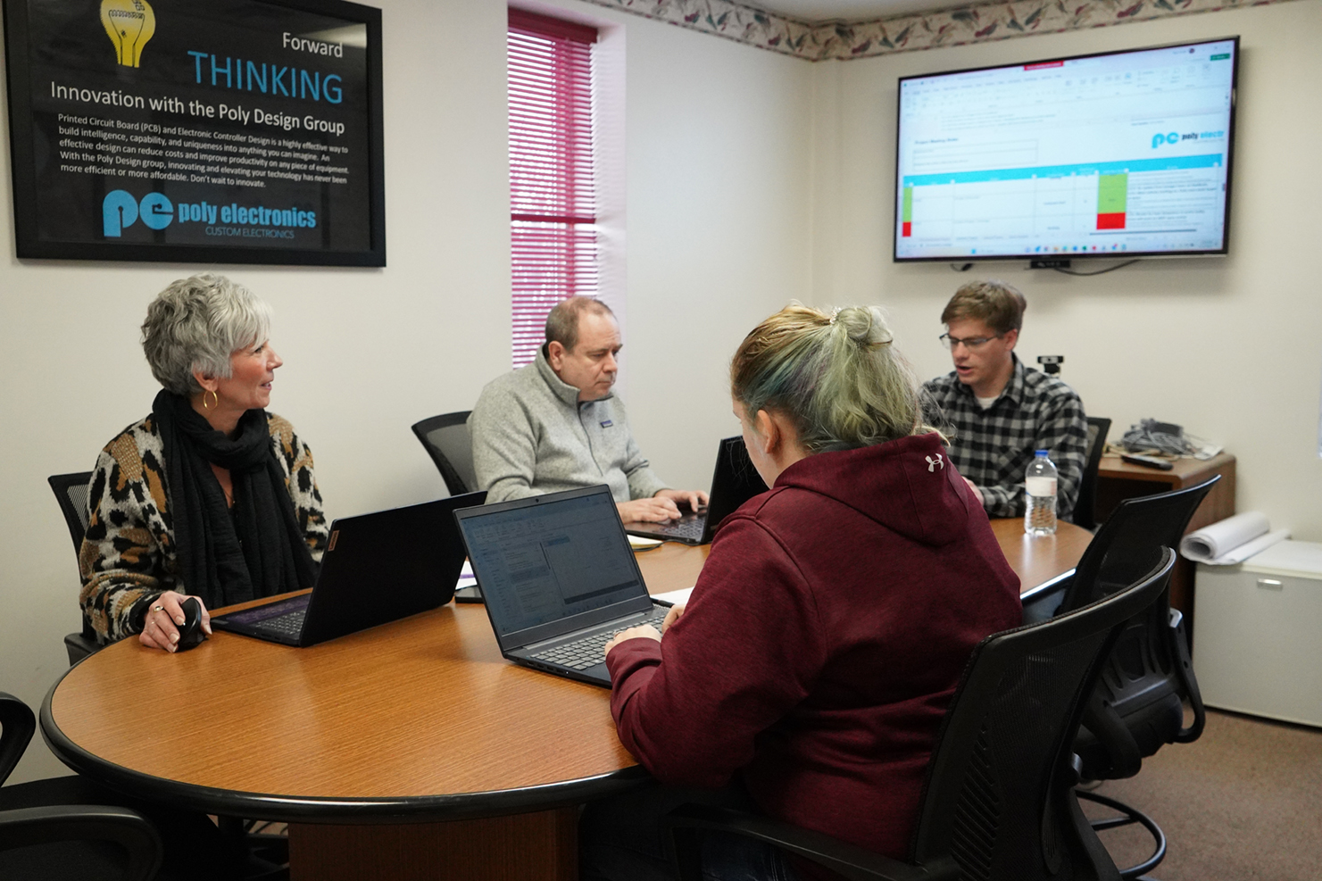
We gladly take the time to meet with you to understand your needs and end goals. Our process begins with listening and provide expert advice to guide you and give you the confidence that you are in good hands.
Step 2: Setting the Bar
Based on what we discussed in our initial meeting, we will turn things over to your project manager to begin outlining goals, functions, and expectations to determine preliminary costs, timelines for development and production, and ultimately, your delivery date for a first batch or full run of finished products.
Step 3: Get the Ball Rolling
Once we’ve set expectations and milestones and agreed upon the price and timeframe, we will promptly start our process of design to ensure your product is delivered on time and on target.
Step 4: Design With Confidence
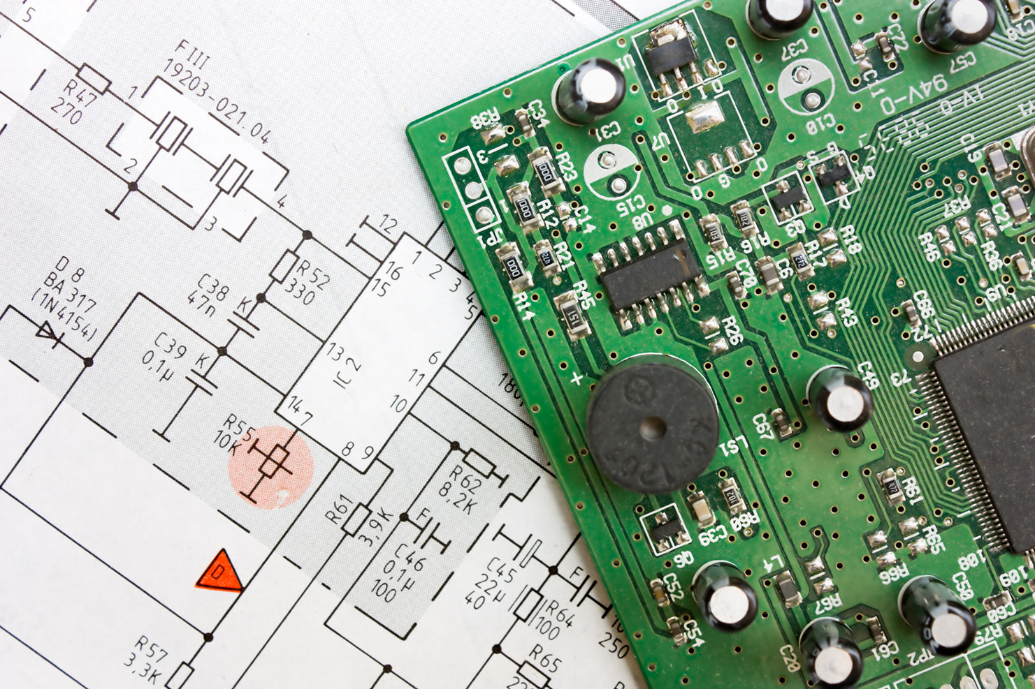
Poly Electronics Design team begins this process by identifying components and reviewing the bill of material with our sourcing department to ensure a cost-effective design and a 100% supply chain risk assessment from the very start.
As the job will be assembled in our facility, we design with our capabilities in mind to ensure a smooth flow from end to end.
Step 5: Prototype & Beta Testing
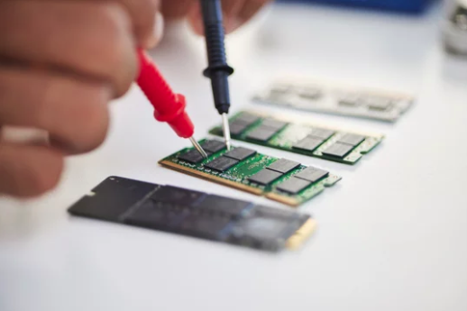
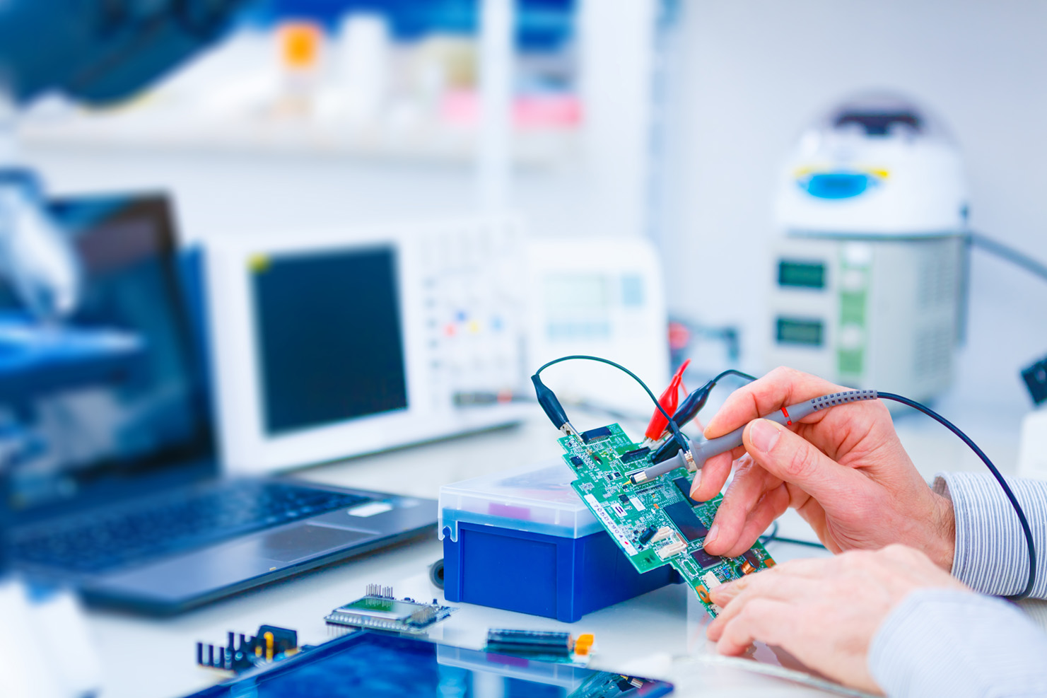
The testing phase of our process proves out what we’ve designed on paper and verifies that the board will work as designed with the electrical current applied.
In many circumstances, we also work with a team to perform visual and functional testing and power-up, burn-in, and environmental testing to detect defects, verify functionality, and evaluate performance under load in a real-world scenario.
The significance of effective PCB testing cannot be overstated. It plays a pivotal role in the early identification and rectification of defects during the manufacturing process. This proactive approach ensures that the final product not only meets quality standards but also performs reliably in the field.
